printed circuit board(PCB), printed board assembly (PCBA)Service hotline:13530785158 Ms. Chen
News
News

Home > News > PCB Process Encyclopedia

PCB Process Encyclopedia
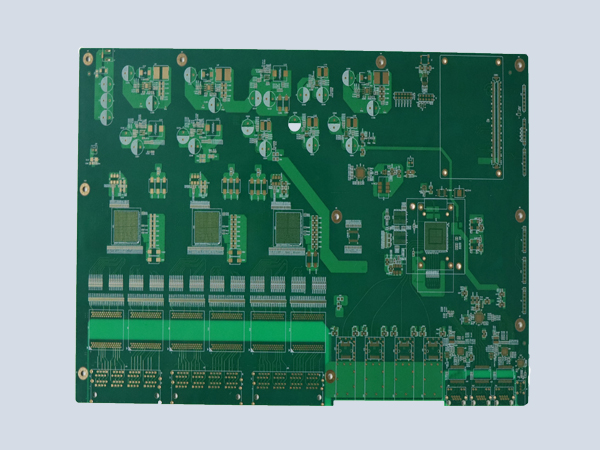
Through hole, blind hole and embedded hole of four layer PCB
Release time:2022-12-13
Via:It is also called through hole. It is completely opened from the top layer to the bottom layer. In a four layer PCB, through holes run through layers 1, 2, 3, and 4, which will hinder the routing of irrelevant layers. There are two main types of vias:
Total 7 record Prev 1 2 Next
Contact Us
Shenzhen Dafengwang Electronics Co., Ltd
Contact: Ms. Chen
Mobile phone: 13530785158

Email: coco@dfwdz.com

Address: 615, Building A, No. 8, Xinhe Avenue, Xinqiao Community, Xinqiao Street, Baoan District, Shenzhen Shenzhenwebsite:www.szdfwpcb.com
Copyright © 2024 Shenzhen Dafengwang Electronics Co., Ltd. 粤ICP备2022148881号