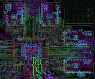
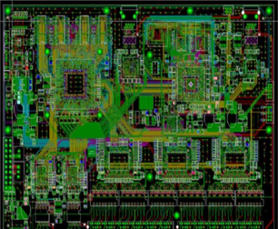
| Maximum design floors | Maximum number of PINs | Maximum connection | Minimum line width | Minimum line spacing | Minimum via | Minimum BGA PIN spacing | Maximum BGA PINs | Highest speed signal |
| 40 | 80000+ | 50000+ | 2mil(HDI) | 2mil(HDI) | 6mil (4mil for laser hole) | 0.33mm | 2500 | 2500 |
| < 3000PIN | 4000-9000PIN | 10000-20000PIN | > 20000PIN |
| 5-7 days | 7-15 days | 16-30 days | Review |
1. PCB processing technology with the highest 64 layers, the minimum line width spacing is 2.5/2.5mil, and the maximum plate thickness aperture ratio is 16:1;
2. The processing technology of long and short gold fingers and the precision control of high-density circuits meet the design requirements of PCB in the field of photoelectric communication;
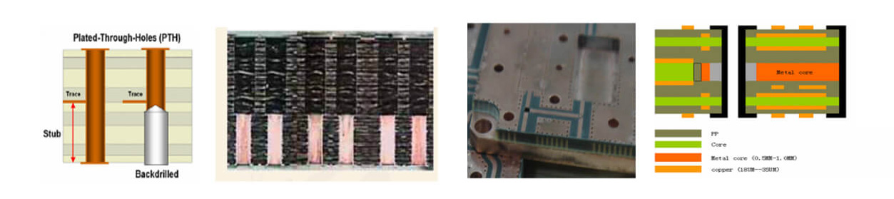
3. High precision back drilling technology reduces the equivalent series inductance of vias and meets the integrity requirements of product signal transmission;
4. Excellent metal base and super thick copper manufacturing process, meeting the high heat dissipation requirements of power supply products:
5. High precision machinery and laser depth control technology, realizing multi-level step groove product structure, and meeting the assembly requirements of different levels of products;
6. Mature pressure mixing process can realize the pressure mixing of FR-4 and high-frequency materials, and save material costs for customers on the premise of meeting the high-frequency performance of products;
7. Advanced Anti CAF technology greatly improves the reliability and service life of PCB products;
8. Priority is given to buried capacitor and buried resistor technology, which greatly improves PCB product performance;
| Highest number of floors | Maximum production size | Minimum line width/spacing | Maximum finished copper thickness | Minimum through hole welding ring |
| 40F | 609*889mm | 2.5/2.5mil | 6oz | 3mil |
| Minimum BGA Pitch | Minimum finished aperture | Maximum plate thickness aperture ratio | Minimum insulation thickness | Minimum BGA pad |
| 0.4mm | 6mil (4mil for laser) | 20:1 | 2mil | 8mil |
| 2-8L | 10-18L | 20-30L | 20-30L |
| 4-8 days | 10-14 days | 15-18 days | 18-22 days |
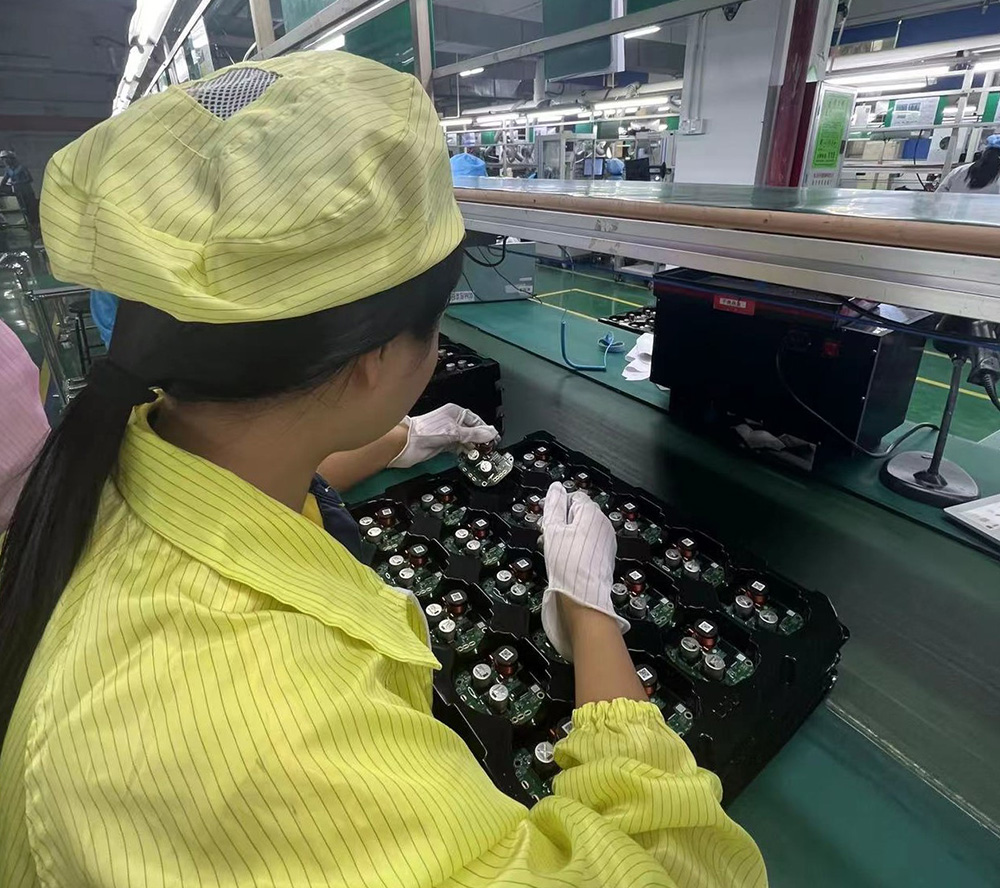
1. UL certification;
2. ISO9001: 2008 Quality System Certification;
3. ISO/TS1694: 2009 system certification;
4. GJB9001B military standard system certification;
5. Huawei/ZTE and other enterprise standards;
6. Manage the processing of customized products in strict accordance with IPC6012II/1l/military standard/customer standard/enterprise internal standard;
7. Strict customer information confidentiality management system.

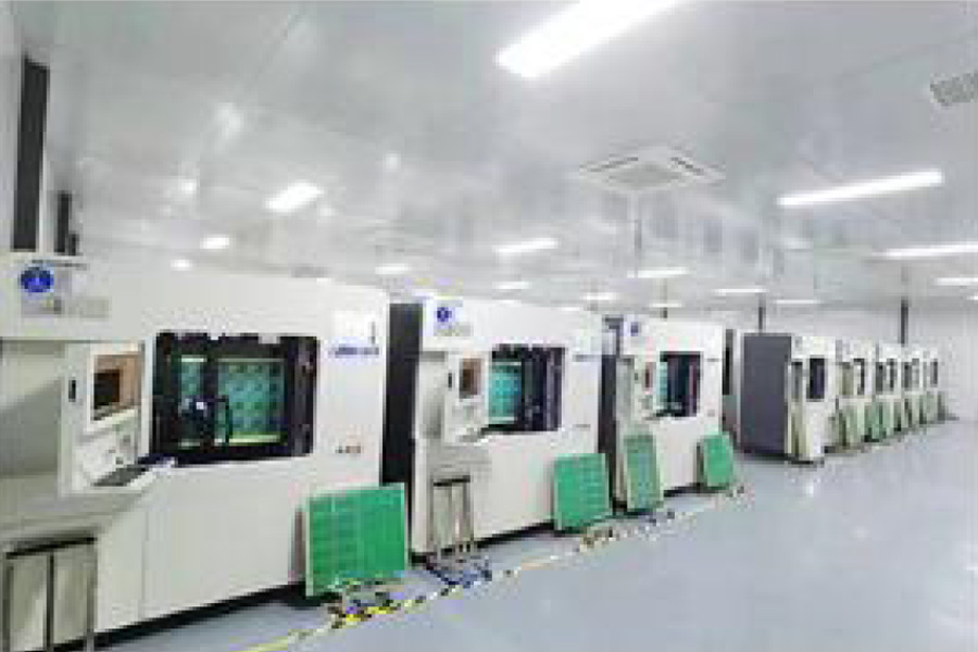
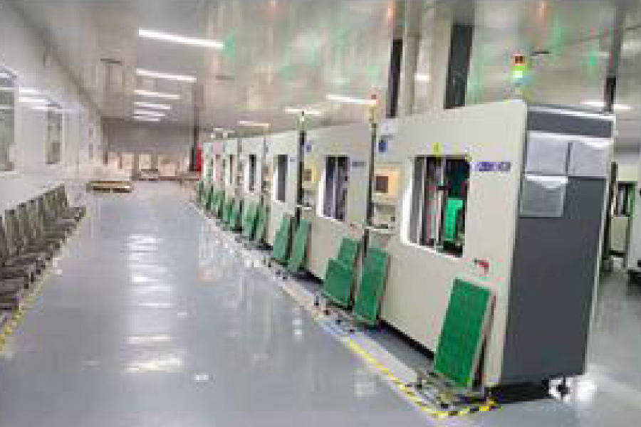
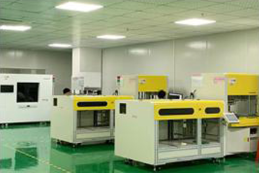
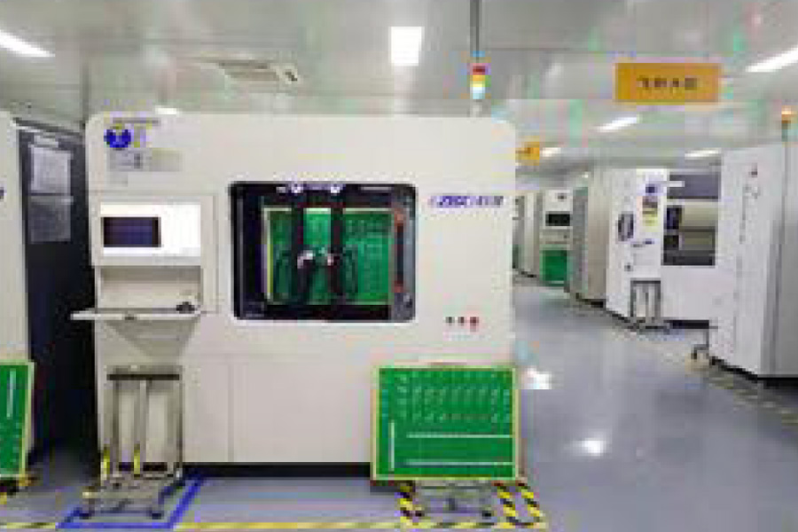
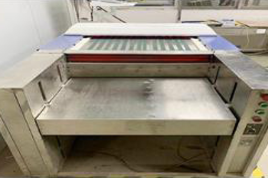
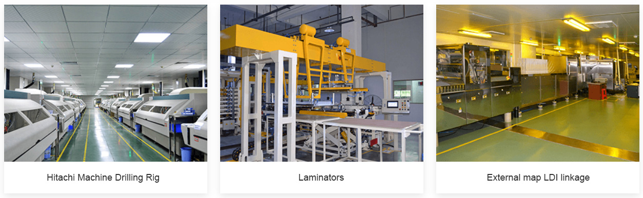
1. Orbotech AOL machine (automatic optical detection) imported from Israel is used to detect increasingly sophisticated PCB products;
2. The high-precision impedance tester imported from the United States meets the impedance test requirements of PCB products;
3. Advanced PLASMA plasma treatment equipment is used for the process of removing glue slag from the hole wall of high-frequency materials such as PTFE and ceramic filler;
4. Ende CNC drilling machine imported from Taiwan is used for processing back drilling and deep hole control;
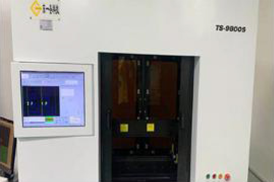
5. Orbotech LDI machine (laser direct imaging) imported from Israel is used for graphic transfer process of high-precision lines;
6. Ende CNC molding machine imported from Taiwan is used for the deep milling process of PCB products with step groove structure;
7. The BURKLE press imported from Germany is used for the pressing process of high-level PCB boards;
8. Vacuum resin hole plugging machine, used for hole plugging process in BGA plate of high precision lines;
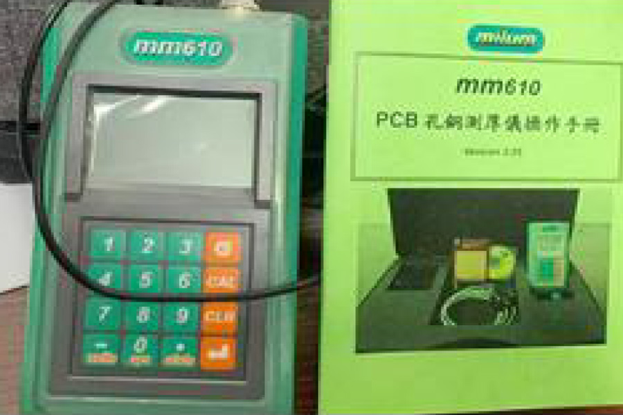
9. A variety of reliability testing equipment, such as ion contamination tester, peel strength tester, hole copper tester, anime tester, gold thickness tester, strongly guarantee the quality of customers' PCB products;
| Technology roadmap | ||||
| Item | 2016 | 2017 | 2018 | |
| Number of Layers | Conventional board | 2-36 | 2-40 | 2-40 |
| Buried IC | no | yes | yes | |
| HDI High density interconnection | 1-2 Rank | 1-4 Rank | 1-5 Rank | |
| Materials | FR4 ( Shengyi ) | yes | yes | yes |
| High Tg | Tg-170 | Tg-210 | Tg-220 | |
| EHalongen Free | yes | yes | yes | |
| High Frequency | yes | yes | yes | |
| Maximum board size | 20*30inch | 20*30inch | 20*35inch | |
| Board thickness | 0.21-6.0mm | 0.21-6.0mm | 0.21-6.0mm | |
| Minimum line width 宽 | 3mil-inner 3mil-outer | 2mil-inner 3mil-outer | 2mil-inner 2mil-outer | |
| Minimum Line gap | 3mil-inner 3mil-outer | 2mil-inner 3mil-outer | 2mil-inner 2mil-outer | |
| Outer layer copper thickness | 5OZ | 7OZ | 7OZ | |
| Inner layer copper thickness | 5OZ | 7OZ | 7OZ | |
| Min. finished hole size (Mechanical) | 0.15mm | yes | yes | yes |
| Min. finished hole size (laser hole) | 0.076mm | yes | yes | yes |
| Aspect ratio | 16 : 1 | 20 : 1 | 20 : 1 | |
| Solder Mask Types and brand | NAYA(LP-4G) | yes | yes | yes |
| Tamura(TT19G) | yes | yes | yes | |
| TAIYO(PSR2200) | yes | yes | yes | |
| Solder Mask Color | green;blue;red;white;black | yes | yes | yes |
| Impedance Control Tolerance | 5% | yes | yes | yes |
| Plug via hole | M in. size can be plugged: | 0.1mm | 0.1mm | 0.1mm |
| Max. size can be plugged: | 0.70mm | 0.70mm | 0.70mm | |
| Min . annular ring can be kept | 3mil | 3mil | 3mil | |
| Min . distance between the IC pads can keep SM bridge | 8mil | 8mil | 8mil | |
| Min. SM bridge for green soldermask | 3mil | 3mil | 3mil | |
| Min. SM bridge for black soldermask | 4mil | 4mil | 4mil | |
| Surface Treatment | H ASL | yes | yes | yes |
| ENIG | yes | yes | yes | |
| OSP | yes | yes | yes | |
| LEAD FREE HASL | yes | yes | yes | |
| GOLD PLATING | yes | yes | yes | |
| IMMERSION Ag | yes | yes | yes | |
| IMMERSIONSn | yes | yes | yes | |
| V-Cut | CNC V-cut, degree | 20\30\45\60 | 20\30\45\60 | 20\30\45\60 |
| V-cut by hand, degree | 20\30\45\60 | 20\30\45\60 | 20\30\45\60 | |
| Outline Profile | CNC | CNC | CNC | |
| Chamfer | T he angle type of the chamfer: | 20\30\45 | 20\30\45 | 20\30\45 |
| Min. distance of jumping chamfer: | 5mm | 5mm | 5mm | |
| Tolerance of the dimension size 外形尺寸公差 | ±0.1mm | ±0.1mm | ±0.1mm | |
| Tolerance of the board thickness | 0.21---1.0 | ±0.1 | ±0.1 | ±0.1 |
| 1.0--2.5 | ±7% | ±7% | ±7% | |
| 2.5-6.3 | ±6% | ±6% | ±6% | |
| Tolerance of the finished hole size | 0-0.3 | +0.08mm | +0.08mm | +0.08mm |
| 0.31---0.8mm | ±0.08mm | ±0.08mm | ±0.08mm | |
| 0.81-1.60mm | ±0.05mm | ±0.05mm | ±0.05mm | |
| 1.61-2.49mm | ±0.75mm | ±0.75mm | ±0.75mm | |
| 2.5-6.0mm | +0.15/-0mm | +0.15/-0mm | +0.15/-1mm | |
| >6.0mm | +0.3 /-0mm | +0.3 /-0mm | +0.3 /-1mm | |
| Certificates(copies are needed) | U L | E360485 | E360485 | E360485 |
| ISO9001 | yes | yes | yes | |
| ISO14000 | yes | yes | yes | |
| ROHS | yes | yes | yes | |
| TS16949 | yes | yes | yes | |
1. Advanced equipment: new imported Sunmsug SMT mounter XPF, NXT3, ten temperature zone lead-free reflux furnace;
2. Professional management team: PCBA senior management team for more than ten years, SMT patch workshop implements Lean Production management;
3. Complete supporting facilities: AOI, SPI, XRAY, SMT patch, post welding and testing;
4. Fast delivery: PCBA project samples will be produced within 3 days, and the 48 hour delivery rate will exceed 96%.
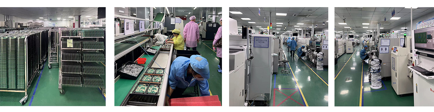
| SMT Capacity | SMT production line | Throwing rate | PCB type | Welding type |
| 2Million+solder joints/day | 2 | 0.25% for passive type; IC class 0% | Conventional hard board/pure soft board/soft hard combination board | Wave soldering, reflow soldering (lead-free/leaded) |
| Minimum package | Minimum device accuracy | Minimum device accuracy | PCB size | PCB thickness |
| 03015 Chip/0.35 Pitch BGA | ±0.04mm | ±O.03mm | 50* 50mm-686*508mm | 0.3-6.5mm |
1. Our company has a team of engineers with three to ten years of experience in electronic component procurement, integrating thousands of high-quality electronic component supply chain resources, providing customers with global procurement services for commonly used electronic materials and major accessories, and reducing customers' material procurement time and cost in the research and development stage;
2. The standardized electronic component supplier certification and annual audit system, strict IQC incoming material inspection, constant temperature and humidity anti-static warehouse storage environment, and in accordance with the "FIFO" material control principle, ensure to provide customers with high-quality electronic component supply services.

Email: coco@dfwdz.com
Address: 615, Building A, No. 8, Xinhe Avenue, Xinqiao Community, Xinqiao Street, Baoan District, Shenzhen Shenzhenwebsite:www.szdfwpcb.com