


 |


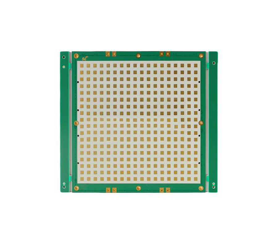
5G test PCB circuit board Shenzhen Dafengwang Electronics Co., Ltd. developed and produced one of the series of 5G communication PCB board, using high-frequency material RO4003C material pure pressure and surface deposition nickel palladium process production. The PCB board is widely used in the field of 5G board testing.
Number of layers:12 layers/14 layers.
Material: high frequency material RO4003C/RO4350B
Board thickness:2.6mm/4..5mm
Surface treatment: surface nickel palladium
Outer layer line width/line spacing: 100/1 00mil or 6/6mil
Minimum hole diameter: 0.4mm
Solder resist character color: white on green
Next:5G IoT PCBs
Email: coco@dfwdz.com
Address: 615, Building A, No. 8, Xinhe Avenue, Xinqiao Community, Xinqiao Street, Baoan District, Shenzhen Shenzhenwebsite:www.szdfwpcb.com


