 |


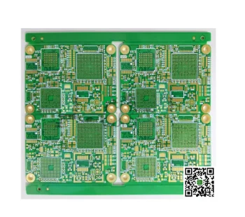
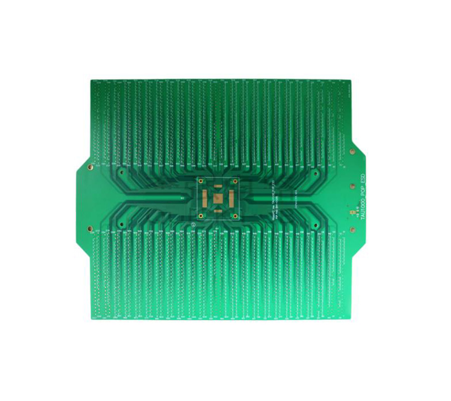
16-layer 7th order semiconductor test PCB board is one of the series of 7th order HDI PCB buried blind hole circuit boards developed and produced by Shenzhen Dafengwang Electronics Co. This type of 7th order HDI buried blind hole circuit board is made of SangYi S1000-2M material, which is drilled and pressed together by laser several times. It is widely used in the field of semiconductor test sinker.
Number of layers:16 layers
Material: Sheng Yi S1000-2M
Board thickness:2.6mm
Surface treatment: submerged gold
Outer layer line width/line spacing:2.2/2.2mil
Minimum hole diameter: 0.1mm
Solder resist character color: white on green
Prev:16-layer, 7-step HDI interconnected PCB with buried blind holes
Email: coco@dfwdz.com
Address: 615, Building A, No. 8, Xinhe Avenue, Xinqiao Community, Xinqiao Street, Baoan District, Shenzhen Shenzhenwebsite:www.szdfwpcb.com