 |


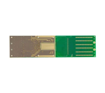
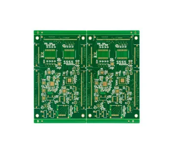
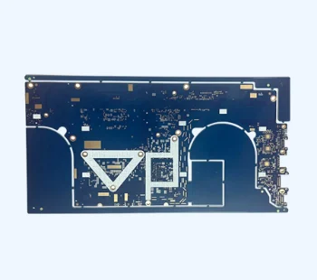
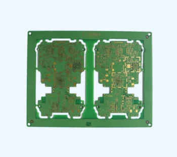
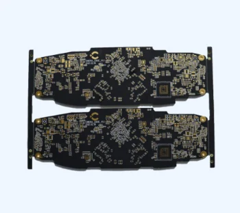
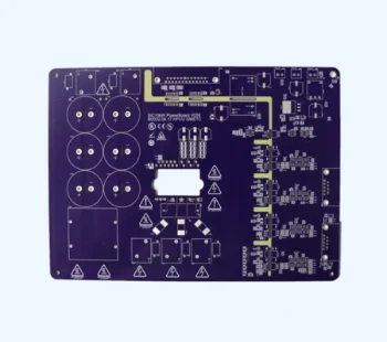
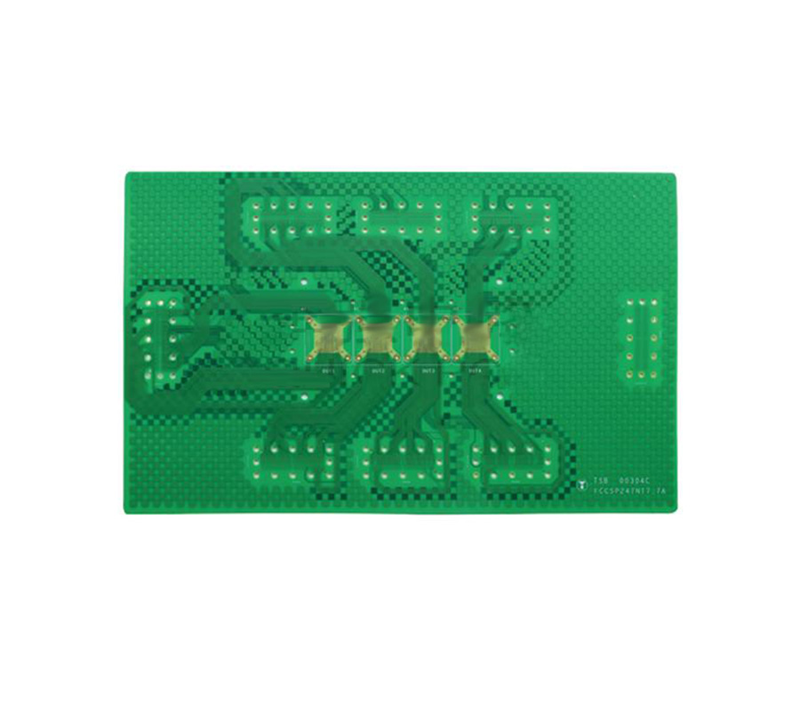
6-layer 2nd order HDI PCB test board, also called 6-layer 2nd order blind buried hole PCB semiconductor test board, is a kind of 2nd order HDI semiconductor test board developed and produced by Shenzhen Dafengwang Electronics Co. The HDI circuit board is made of SangYi S1000-2M substrate, and after the PCB manufacturing process such as laser drilling and surface gold plating, the aperture can reach 0.1mm and the line width/line spacing can reach 75/75um, and the product is widely used in semiconductor test field.
Number of layers:6L
Material:S1000-2M
Plate thickness:2.0mm±0.15mm
Copper thickness:1oz
Surface treatment:sunken gold 2u"
Outer layer line width/line spacing:75um/75um
Minimum hole diameter:0.1mm
Solder resist character color: green oil white character
Email: coco@dfwdz.com
Address: 615, Building A, No. 8, Xinhe Avenue, Xinqiao Community, Xinqiao Street, Baoan District, Shenzhen Shenzhenwebsite:www.szdfwpcb.com