printed circuit board(PCB), printed board assembly (PCBA)Service hotline:13530785158 Ms. Chen
Products
Products

Home > Products > Multi-rise PCB > High Level PCB Boards (12L-60L)

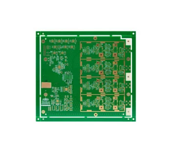
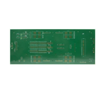
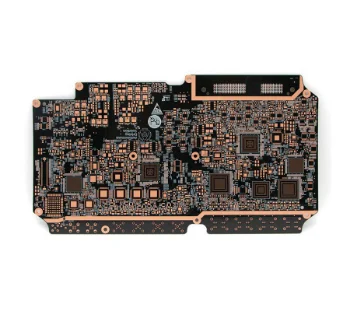
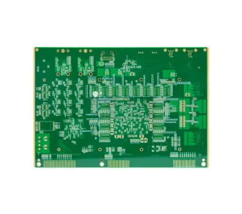
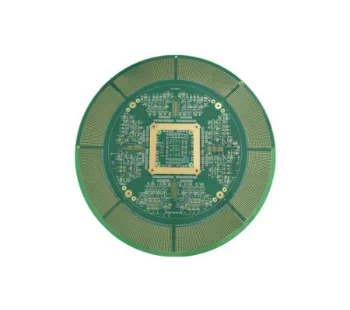
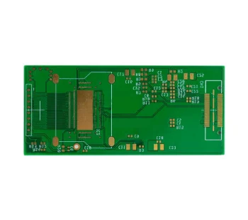
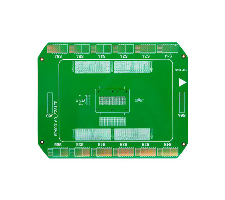
14 layer high aspect ratio semiconductor test thick gold plate
  • 14 layer high aspect ratio semiconductor test thick gold plate
  • 14 layer high aspect ratio semiconductor test thick gold plate
14 layer high aspect ratio semiconductor test thick gold plate

14-layer high thickness to diameter ratio semiconductor test thick gold board is a series of semiconductor test high level PCBs developed and produced by Shenzhen Dafengwang Electronics Co.

Layer:14L


Material: raw benefit S1000-2M


Plate thickness:5.0mm+0.5mm


Copper thickness:1oz


Surface treatment: gold plated 5u"


Outer layer line width/line spacing:100/90um


Minimum hole diameter: mechanical hole: 0.35mm plate thickness hole diameter ratio: 14:1


Solder resist character color: green oil white character


Prev:12 layer RF PCB circuit board

Next:16 layer gold plated semiconductor test board

Contact Us
Shenzhen Dafengwang Electronics Co., Ltd
Contact: Ms. Chen
Mobile phone: 13530785158

Email: coco@dfwdz.com

Address: 615, Building A, No. 8, Xinhe Avenue, Xinqiao Community, Xinqiao Street, Baoan District, Shenzhen Shenzhenwebsite:www.szdfwpcb.com
Copyright © 2024 Shenzhen Dafengwang Electronics Co., Ltd. 粤ICP备2022148881号